IMAGE PROCESSING SYSTEM
Semiconductor manufacturing equipment images
HTL has refined its image processing technology through the development of semiconductor manufacturing equipment over many years.
Semiconductors require microprocessing, and images captured by a camera through a high-magnification lens are used to perform processing and check the processing results.
The images captured by a camera through a high-power lens are used to perform processing and to check the processing results. However, if the image is unclear, processing is required to improve visibility (ease of viewing).
Image processing technology is used for this purpose.
Image processing system
Based on this experience, we have realized and provided unique image processing algorithms, such as speed enhancement and image enhancement, to meet the various needs of equipment that handles images.

Example of Image Processing for Semiconductor Manufacturing Equipment
(1)Improved visibility (a world of tens of nm that elicits the critical performance of H/W)
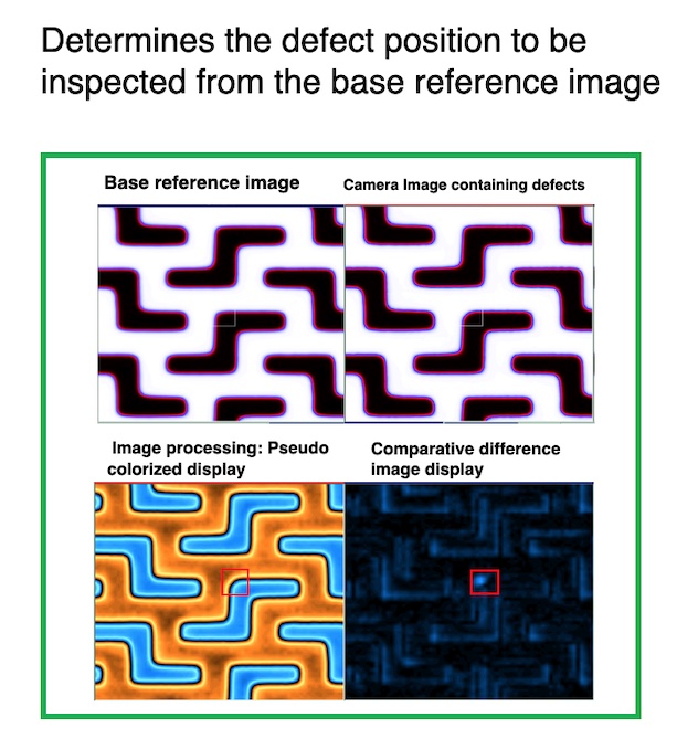
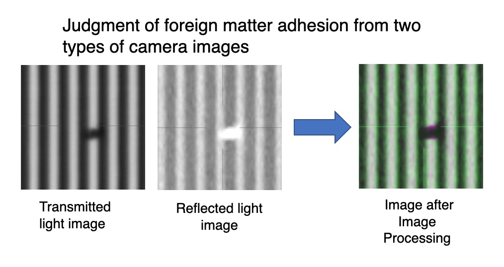
Contrast enhancement, noise removal, pseudo-color display, etc.
(2)Auto Focusing (high accuracy automatically)
(3)Edge lock (high-precision machining)
(4)Pattern copy assist (operation assist using repeated information)
(5)Pattern matching (automatic detection of position, determination of shape, etc.)

Consultation・Estimate
CONTACT

※You can use our contact form or call us.